

EE 230 PMOS – 1
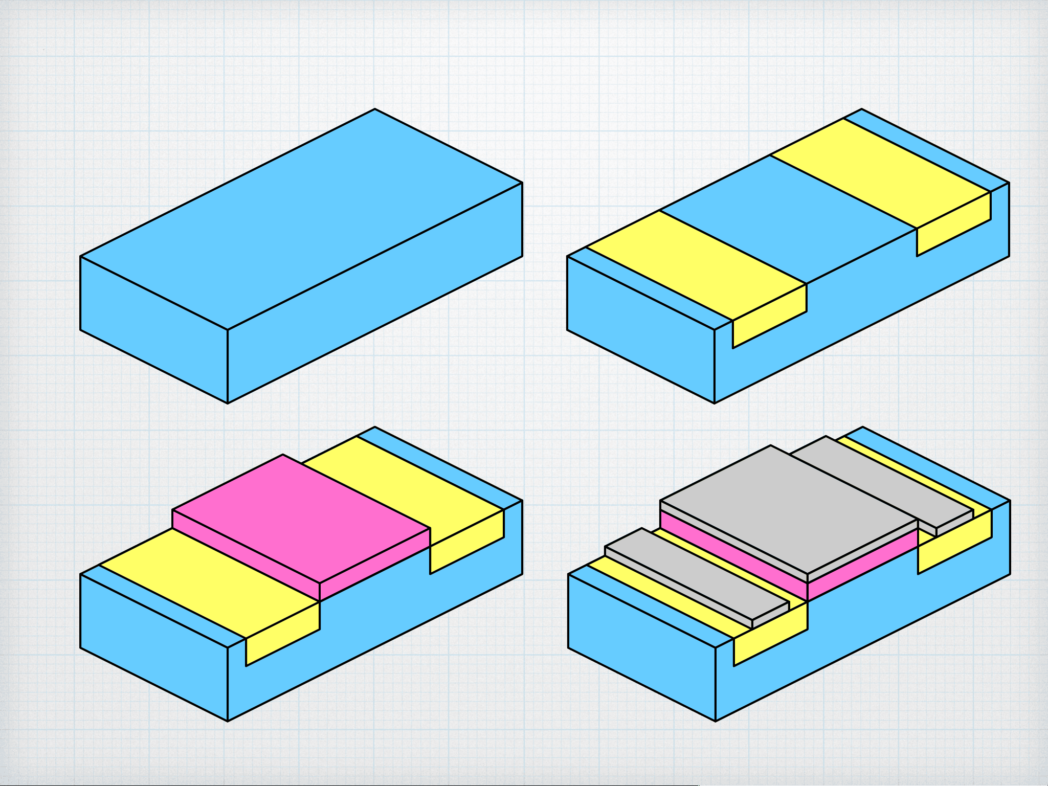
n-type substrate p-type source
& drain
gate oxide
metal contacts
Basic PMOS structure
p-channel device (n- and p-type regions reversed.)
oxide
width (W)
oxide
gate


Study with the several resources on Docsity

Earn points by helping other students or get them with a premium plan

Prepare for your exams
Study with the several resources on Docsity
Earn points to download
Earn points by helping other students or get them with a premium plan
Community
Ask the community for help and clear up your study doubts
Discover the best universities in your country according to Docsity users
Free resources
Download our free guides on studying techniques, anxiety management strategies, and thesis advice from Docsity tutors
An in-depth analysis of PMOS (P-channel Metal-Oxide-Semiconductor) transistors, including their basic structure, critical dimensions, operation principles, and equations. PMOS is a p-channel device with n- and p-type regions reversed compared to NMOS. topics such as the PMOS capacitor, hole inversion, threshold voltage, and the i-v curve.
Typology: Exams
1 / 20

This page cannot be seen from the preview
Don't miss anything!
n -type substrate
p -type source
& drain
gate oxide
metal contacts
p -channel device ( n - and p -type regions reversed.)
oxide
width (
W )
oxide
gate
gate length (distance from source
to drain) – currently
as small as 20 nm.
width: typical L to 10 L
( W/L ratio is important)
oxide thickness: typical 1 - 10 nm.
width (
W )
oxide
gate
length (
L
)
oxide thickness ( t ox
)
source
drain
width (
W )
Same as the NMOS capacitor, but with n -type substrate.
In the substrate, there are lots of electrons (majority carriers), and
relatively few holes (minority carriers).
ox
body gate
contact
substrate (body)
Apply a positive voltage
to the gate – electron
accumulation.
Apply a (smallish)
negative voltage to the
gate. Electrons are pushed
away and a few holes are
attracted – carrier
depletion.
v GB
body gate
contact
substrate (body)
v GB
body gate
contact
substrate (body)
v
GB
electron accumulation
T
< v
GB
carrier depletion
v
GB
T
inversion –
hole sheet forms.
(Note: V T is negative.)
Through the application of the gate voltage, we can control what is
happening with carriers under the gate.
Creating a hole inversion layer connects the source to the drain. The
PMOS is “on”.
For now, we connect the source to the body and apply the controlling
voltage between the gate and the source. This is OK for the time
being, but we will have to revisit the issue of the body connection
later. With the drain also at ground, the inversion layer (channel) is
uniform between source and drain.
i D
electrons drain
source
gate
n
p p
v GS
T
hole inversion layer
body
If v DS is kept small, the current flow is
“ohmic” – like a resistor. R DS depends on
the how much gate voltage is applied
(determining the hole concentration in
the inversion layer) and the physical
dimensions of the PMOS.
i D
v DS
DS
v DS
i D
holes
drain
source
gate
n
p p
v GS
T
hole inversion layer
body
v DS
i D
holes
drain
source
gate
n
p p
v GS
T
hole inversion layer
body
But as v DS becomes more negative, the
hole concentration at the drain is reduced
is becoming more resistive. The i-v curve
becomes non-linear, becoming parabolic.
i D
2 ( v GS
T
) v DS
� v
2
DS
μC ox
v GS
T i D = 0 off
v GS
T
_v DS
v GS_
T
i D = K [ 2 ( v GS
T ) v DS
- v DS
2 ]
ohmic or
linear
v GS
T
v DS < v GS
T
i D = K [ v GS
T
2 saturation
μC ox
T
Note the equations are identical
to the NMOS equations. For a
PMOS, v GS and v DS are both
negative and the current flows
from source to drain.
In applying the drain voltage to make the drain current flow, why did we
use a negative value for v DS ? It would seem that a positive v DS would be
The reason becomes clear when we consider the p-n junction formed by
the drain and the substrate.
If the substrate is at ground potential and we apply a positive voltage to
the drain, the p-n junction there would be forward-biased – probably
with a very large voltage – and huge currents would flow from the drain
into the substrate. The junction would likely be burned out.
The PMOS substrate rule: The substrate (body) should be connected to
the highest voltage in the circuit – usually the positive power supply.
Then the source and drain must both be at the same or lower voltages,
and it will be impossible to forward-bias the diodes.
v DS
i D
holes
drain
source
n
p p
v GS
T
hole inversion layer
body
v GS
v DS
i D
DD
D
G
10 kΩ
Kp = 0.5 mA/V
2
Essentially the same circuit but with a different
value of RD.
From the previous examples, we can be certain
that the PMOS is on. Guess saturation again, and
we get the same value for the current.
i D
p (
v GS
Tp )
2
0.5 mA/V
2
2
= 4.5 mA
v DS
DD
4.5 mA ) (
10 kΩ )
Oh no! The drain-to-source voltage is not more negative than VGS – VT ,
so it can’t be in saturation. In fact, 35 V is not even possible given the
power supplies. The PMOS must be operating in ohmic.
i D
p [
GS
Tp )
DS
2
DS ]
v DS
DD
D
i D
v DS
DD
D
EE 230 PMOS – � 17
v DS
DD
D
p [
GS
Tp )
v DS
− v
2
DS ]
Blerk!
Plug into your calculator and solve. Or do it the old-fashioned way —
start by re-arranging:
v
2
DS
GS
Tp )
p
D
v DS
DD
p
D
Plug in values:
v
2
DS
{
2 [
− 4 V − (− 1 V) ]
−
1
(
0.5 mA/V
2
) (
10 kΩ )
}
v DS
−
− 10 V
(
0.5 mA/V
2
) (
10 kΩ )
= 0
v
2
DS
v DS
2
= 0
Equating the resistor current to the drain current:
Solve to get vDS = –0.341 V or vDS = –5.86 V. The larger value is not
consistent with the PMOS being in ohmic. So with vDS = –0.341 V, the
drain current is:
i D
v DS
DD
D
10 kΩ
= 0.97 mA
v GS
v DS
i D
DD
D
With NMOS transistor, we saw that if the gate is tied
to the drain (or more generally, whenever the gate
voltage and the drain voltage are the same), the
NMOS must be operating in saturation. The same is
true for PMOSs. In the circuit at right, vDS = vGS ,
and so vDS < vDS – VTp will always be true for VTp < 0.
With the PMOS in saturation:
i D
p (
v GS
Tp )
2
p (
v DS
Tp )
2
and,
v DS
= i D
D
DD
Insert the second into the first:
i D
p (
i D
D
DD
Tp )
2
Expand:
i D
p [
i
2
D
2
D
DD
Tp )
i D
DD
Tp )
2
1 kΩ
Kp = 0.5 mA/V
2
Re-arrange:
i
2
D
DD
Tp )
D
p
2
D
i D
DD
Tp
D
2
Plug in values:
i
2
D
−
2 [
10 V + (− 1 V) ]
1 kΩ
1
(
0.5 mA/V
2
) (
1 kΩ )
2
i D
[
10 V + (− 1 V)
1 kΩ
]
2
= 0
i
2
D
− ( 20 mA) i D
2
= 0
Solve to give: iD = 5.64 mA or iD = 14.36 mA. The larger voltage is too
big — in that case vDS = +4.36, which is not compatible for a PMOS.
So the drain current is iD = 5.64 mA and the corresponding drain-to-
source voltage is vDS = –4.36 V. All is good.